
 During my minimalistic solar powered datalogging project (here, here and here) I was at the point where I had more data than could be stored in my 32KB EEPROM. It was time to have more! As I already had the 24AA256 (32KB) from Microchip because of the wide supply voltage range and the low power consumption I looked for the biggest one of this series: The 24AA1025 is a 128KB EEPROM! It’s pins A0 and A1 can be used to address more than one chip. So there is a maximum of four chips giving you a total of 512KB EEPROM for your ATmega328P. This post describes the hardware setup (easy) and the software side. In the end we have a 512KB EEPROM memory with linear address range.
Hardware setup
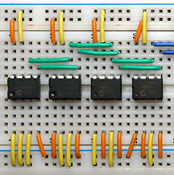
This picture shows the total setup:
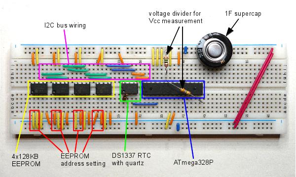
The setup contains the ATmega328P, a RTC for timing and a supercapacitor as the energy source. The memory is made of 4x24AA1025. They are connected to the ATmega via I2C bus.
Microchip Technology Inc.
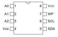
The pinout of the 24AA1025 looks the same as of the 24AA256 but not all pins have the same function. Pins A0 and A1 can be used to select one of four chips. The individual I2C addresses can be encoded via these pins. On the 24AA256 this happened with pins A0 through A2 giving a maximum of 8 individual chips. Pin A2 of the 24AA1025 must be always HIGH. Otherwise the chip doesn’t work at all (same function as a Chip Select pin). In the picture above the EEPROM address setting can be seen for the four chips: A1 (pin 2), A0 (pin 1) being 00, 01, 10, 11 from right to left. A2 (pin 3) is always 1.
Write Protect (pin 7) is always 0 to enable writing the memory.
The I2C bus, SCL (pin 6) and SDA (pin 5) is connected through all I2C devices including the RTC and to Analog Input 5 (pin 28) and Analog Input 4 (pin 27) of the ATmega328P. This is the standard wiring giving full functionality with the Wire.h library of the Arduino IDE. As Wire.h uses the pullup resistors of the ATmega328P for the I2C bus no external pullups are necessary.
Addressing the memory
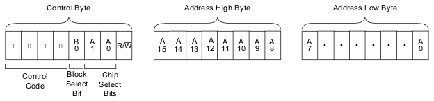
Addressing a byte in the memory is writing three bytes to the chip via I2C:
Microchip Technology Inc.
The left seven bits of the control byte form the I2C address. Bits A0 and A1 must match the hardware settings of pins A0 (pin 1) and A1 (pin 2). This is the same as with the smaller 24AAxxx EEPROMs.
Addressing a single byte inside the memory of a chip is done by the following two bytes: Address High Byte and Address Low Byte giving a total of 16 address bits and thus, an address range of 65536 bytes of memory. But the 24AA1025 has 131072 bytes! They cannot be addressed with only 16 bytes. Therefore the total memory space is divided in two blocks of 65536 bytes each. Selecting one of the two blocks is done with the Block Select Bit of the Control Byte.
In practice this means that in one chip there are two 64KByte blocks that are addressed with two different I2C addresses (Block Select Bit 0 or 1). So when you have A0 and A1 tied to 0 your lower memory block of the chip is at address 0x50 and the higher one at 0x54. The address of the higher block is: address of lower block + 4. This makes it rather confusing when you have more than one chip:
E. g. with two chips (the two on the right side of the above picture) you will have the following addresses:
Chip 0: A0 = 0, A1 = 0: low block at 0x50, high block at 0x54
Chip 1: A0 = 1, A1 = 0: low block at 0x51, high block at 0x55
With four chips the situation is:
Chip 0: A0 = 0, A1 = 0: low block at 0x50, high block at 0x54
Chip 1: A0 = 1, A1 = 0: low block at 0x51, high block at 0x55
Chip 1: A0 = 1, A1 = 0: low block at 0x52, high block at 0x56
Chip 1: A0 = 1, A1 = 0: low block at 0x53, high block at 0x57
Here, all addresses from 0x50 through 0x57 are used but not all the memory physically is at the place you would expect it by only seeing the addresses.
Making a linear address range
The idea is to have a variable (let’s call it address 😉 ) that contains the address of the byte we want to access and we don’t have to care in which physical device this byte resides. Yeah, I think this is what is called memory management. So let’s build a memory management unit on the ATmega328P for our I2C memory chips! Let’s look at the code that makes the translation:
#include <Wire.h>

// Variables for memory management with 24AA1025
// block[] maps the number of the present memory block to I2C addresses
// One 24AA1025 has two blocks with 65536 bytes each.
int block[] = { 0x50, 0x54, 0x51, 0x55, 0x52, 0x56, 0x53, 0x57 };
int numberofblocks = 8;
First of all, we need Wire.h for I2C communication. Then we make an array with the I2C addresses of the individual 64KB blocks. The order of the addresses represents the order the different blocks are accessed: Lower and upper block of chip 0, then lower and upper block of chip 1 and so on. The index of the array forms the upper 3 bits of our address (bits 16 to 18).
When we read or write data through a loop we need to know where the address range starts and ends:
// EEPROM address range
unsigned long EEPROM_start_address = 0;
unsigned long EEPROM_end_address = (65536 * numberofblocks) -1;

// linear EEPROM address
unsigned long address = 0;

// data that is read or written
byte data = 0;
EEPROM_start_address and EEPROM_end_address are the addresses of the first and the last byte of our total EEPROM memory. Then, the address itself is defined and also a byte value to hold the data that is read or written.
Now we want to write a byte to our memory:
// write one byte to EEPROM
// set I2C address and send two address bytes
Wire.beginTransmission(byte(block[address / 65536]));  // get I2C address
Wire.write(byte((address % 65536) / 256));             // EEPROM adress high byte
Wire.write(byte((address % 65536) % 256));             // EEPROM adress low byte
// send data byte
Wire.write(data);
Wire.endTransmission();
Wire.beginTransmission forms the Control Byte (see above) from the 7-bit I2C address. From our linear (19-bit) address we separate the upper three bits by simply dividing through 65536 = 216. This gives us the index for calling the block[] array. We come back with the according I2C address and give it to Wire.beginTransmission.
Then, with modulo division of address we get the lower 16 bits of the address. This is then separated in two bytes ( high byte and low byte) in the same manner.
Now we have sent the I2C address of the block we want to write to and also the 16-bit address of the individual memory cell. Next is to send our data byte. Wire.endTransmission writes everything to the EEPROM in one flush and then terminates the write process. Note that after a write you have to wait around 5 milliseconds until the next write to give the EEPROM enough time to finish it’s internal write procedure. Otherwise the next data will be lost.
Reading a byte is as follows here:
// read one byte from EEPROM
Wire.beginTransmission(byte(block[address / 65536]));  // get I2C address
Wire.write(byte((address % 65536) / 256));             // EEPROM adress high byte
Wire.write(byte((address % 65536) % 256));             // EEPROM adress low byte
Wire.endTransmission();

Wire.requestFrom(block[address / 65536],1);
if (Wire.available()) data = Wire.read();
The byte is addressed in the same way as above. After sending the complete address the write cycle ends and then reading begins with requesting one byte from the same I2C device. When data is available it is read.
These examples show the very basic code for read and write. As the EEPROMs are rather slow in write mode it makes sense to use block mode where up to 128 bytes can be written at once. Let’s talk about this in another post…
Conclusion
512KB EEPROM can be connected to the ATmega328P via I2C. This memory is physically organized in blocks of 64KB. To have a linear address range the upper bits of the linear address are translated into the I2C addresses of the individual blocks. This way we get a monolithic memory range of 512KB = 524,288 bytes of EEPROM memory.
Enjoy
heliosoph